Tuesday, November 12, 2024

500 Watt Antenna Tuner Part 9 - Pre Build Schematics and Board Layout

 I am getting ready to order parts and build the tuner.  To prepare for it, I have updated the blog.  

I am planning to package the tuner on an open breadboard to showcase its construction.  It will be composed of three components (like the early prototype picture that I included in the matching algorithm page).  The three components are the directional coupler, the tuner controller and the RF deck.  

Here are the pages of the tuner controller:


Main/Microcontroller Page


Attenuator/Measurement Page


Controller Board Layout


And here are the pages for the RF Deck:


Main/Interconnect Page


Sunday, November 10, 2024

500 Watt Antenna Tuner Part 8 Software and Microcontroller

 Controller Hardware and Programming Language Selection

This is a new iteration of this page.  I have kept the old page and included it at the end of this blog post series for anyone interested.

With the recommendation of a friend, Mike Rauch K2VPX, I started looking at the Raspberry Pi Pico.  I built a test frequency generator and the frequency measurement function for this tuner.  It worked well and I really liked what I saw.  The documentation is superb.  I also chose its native C programming environment for no other purpose than to keep things as simple as possible.

I also tested an interface between the Raspberry Pi Pico and the Mac over USB and I am satisfied that it works reasonably well.

To conserve pin count and keep the board layout simple, I have chosen the SPI interface and tested the software for driving it.  I am using three NCV7240ADPR2G relay drivers.  I have also decided to put the 3 relay drivers in series as shown by the data sheet.  The Raspberry Pi Pico SPI Chip Select pin makes a low to high transition at the end of each block of data, so it does not meet the requirements of cascading the three relay drivers.  The workaround is to operate the CSN pin software separate from the data transmission using the SPI library.  Here is the pin utilization for the microcontroller

  • 4 pins for the SPI interface.  I am using SPI1 and specific pins to make the board layout easier.
    • RX: GPIO12 (note, GPIO, not pin numbers)
    • CSN: GPIO13
    • SCK: GPIO14
    • TX: GPIO15
  • 2 analog pins for magnitude and phase of the reflection coefficient
    • Phase: GPIO26_ADC0
    • Magnitude: GPIO27_ADC1
  • 1 analog pin for power level input
    • Power: GPIO28_ADC2
  • 1 pin for frequency input
    • Frequency: GPIO10
  • 1 pin for gating the frequency measurement (so I am not shipping a high frequncy digital signal all over the printed wiring board)
    • Measure: GPIO11
Lot's of spare pins left.  The 12 bit A/D convertors and fast floating point arithmetic are both pluses.   But the true winners are the documentation and the SDK.

Design Concepts

My core design idea is to interface the tuner to my Stationmaster software and use its ability to manage the radio, the linear, and the tuner together.  As of right now, I don't have any concrete ideas for a local display.  I might just stick with setting limits on power and SWR and Power measurements and lighting a red LED.  Then the Stationmaster software can interrogate the tuner and display the results.

The Stationmaster software will be interfaced with the Pico over the USB interface.  The commands from the Stationmaster to tuner are formatted as follows:
  • Address (one byte)
  • Command (one byte)
  • Data bytes as needed (zero or more bytes)
  • Terminating semicolon ";" (one byte)
Other than the address byte, this is the same format as the Yaesu radio commands.

The replies to the commands will be formatted as follows:
  • Address (one byte) 
  • Command (one byte) - the same as the command received
  • Data bytes as needed (zero or more bytes) 
  • Terminating semicolon ";" (one byte)
There will be two sets of commands.  One set for normal operation and another set for testing of the tuner.

Operating Commands:
  • Test tuner (to see if the device at this USB port is the tuner) - returns Address, Command, ;
  • Bypass - returns Address, Command, (decrease power or done - one byte), ;
  • Measure power - returns Address, Command, two bytes of data,;
  • Tune - returns Address, Command, (decrease power, increase power, or done), ;
Testing Commands:
  • Read phase - returns Address, Command, two bytes of data, ;
  • Read magnitude - returns Address, Command, two bytes of data, ;
  • Read frequency - returns Address, Command, four bytes of data, ;
  • Read digits (of the A/D convertors) - returns Address, Command, two bytes of data, ;
  • Read volts (of the A/D convertors) - returns Address, Command, two bytes of data, ;
  • Read LC (for positive and negative phases) - returns Address, Command, four bytes of data,;
One of the challenges with this program is to make sure that the code is readable and maintainable and that is when this objective runs into the other objective which is to make for making the board layout as easy as possible.  That resulted in a completely random assignment of capacitor and inductor relays to relay driver pins from the sofware point of view.  The routing of the bits out of the microcontroller to the relay drivers is as follows (for IC numbers, see the schematics in the next section).
Microcontroller => IC3 => IC1 => IC2 => Microcontroller 
So the first 16 bit word that is shipped out drives the pins to IC2, the second word drives the pins in IC1 and the third word drives the pins in IC3.  Here is what I think will make the code easy to read and maintain.

  struct relay{
  	int wordNo; //word 0 to IC2, word 1 to IC1 and word 2 to IC3
  	int pos;    //positiion of the two bits driving the relay
  };
  
  struct relay capRelays[8] = 
  	{
    	{2, 5},
        {2, 3},
        {2, 2},
        (1, 6},
        {1, 4},
        {1, 2},
        {1, 1},
        (0, 6},
    };
    
  struct relay indRelays[8] = 
  	{
    	{0, 3},
        {0, 4},
        {0, 5},
        {1, 0},
        {1, 3},
        {1, 5},
        {1, 7},
        {2, 4},
    };
    
  struct relay bypass[2] =
    {
    	{2, 6}, //input
        {0, 0}, //output
    };
    
  struct relay caps[2] =
    {
    	{2, 7}, //input
        {0, 7}, //output
    };
    
  struct relay comps[2] =
    {
    	{0, 2}, //series capacitor, close to short
        {0, 1}, //shunt inductor, close to engage
    };
  uint16_t words[3] = {0x0000, 0x0000, 0x0000}

The approach will be to locate the "1" position in the relay or capacitor position byte (outcome of the tuning algorithm), index into the capRelays or indRelays respectively, then pick the word number and change the bit positon as indicated by the relay driver datasheet. At least for now, my plan is to change on relay position at time with a little bit of delay between the changes to minimize noise.

To convince myself that the serial connection of the relay drivers works and also to debug the software for driving the relays, I am building a prototype board of the Raspberry Pi Pico, the three relay drivers and a bunch of LEDs and two relays.  It also gives me a chance to test the 5 volts feed circuit that I did not test in my previous prototype build.  Here it is.


I add more documentation to the code and link the Github page.


Wednesday, November 6, 2024

500 Watt Antenna Tuner Part 4B Inductor Design

 One of the design challenges that Jeff, K6JCA outlines in his blog is stray inductance of the connecting wires or PCB tracks.  He used hand wiring in his construction, so I thought I might do better with a PCB layout.  I went through a design cycle with six air wound inductors and two powdered iron core inductors and did a few design iterations of the PCB with KiCad.  I did not build the board but extracted the board geometry and estimated the path inductance.  My results were the same as Jeff's.  

I decided to build all my inductors with toroid cores.  This provides me the advantage of packing them closer to each other and help keep the connecting tracks shorter and hence reduce the path inductance.  This is the approach that some of the commercial high power antenna tuners take.

Also, I noticed that some of the commercial high power antenna tuners placed the capacitor and inductor relays on the back side of the board (the same with Jeff's design).  This approach tends to further reduce the path inductance without increasing the PCB cost since I am using through hole relays and calling for solder mask on both sides of the board.  

For high power inductors, the recommended material to use is powdered iron cores (not ferrite), so that is what I will use.

The Mini Ring Calculator for Mac is now available, but I am familiar with the Micrometals on line tool, so, that is what I will use.  I will assume an internal enclosure temperature of 50 degrees C and maximum core temperature increase of 50 degrees C.  That meets the maximum toroid core temperature of 100 degrees C which is fine for intermittent use.  The other factor that I need is the maximum RMS current through the inductor at each frequency.

My simulator (described earlier), calculates maximum current through the inductors and maximum voltage across the inductors, but not the current at maximum voltage.  Fortunately, knowing the maximum voltage, I can calculate the current at this voltage with a spreadsheet.  

The following table is the simulator output that shows peak inductor currents and peak inductor voltages across the HF bands at average 200 watts operating power. 

Ind Current12.8 uH6.4 uH3.2 uH1.6 uH800.0 nH400.0 nH200.0 nH100.0 nH50.0 nH25.0 nH
160m low8.94674422981618140201053
160m high8.904583221789045221163
80m low8.90474437292157783920105
80m high8.900458322178904522116
40m low8.90047443729215778392010
40m high8.90045344430116382412010
20m low8.9000474437292157783920
20m high8.9000466440297160804020
17m low8.900004683512001015125
17m high8.900004713512011025125
15m low8.900004843832291185929
15m high8.900004793862331206030
12m low8.900004814152651397035
12m high8.900004834172661407035
10m low8.900004744372911577839
10m high8.900004724463051668342
6m low8.90000048341726614069
6m high8.80000047643328315075
Max8.946747447447448448343328315075
Max RMS6.3330.2335.2335.2335.2342.2341.5306.2200.1106.153

Inductor Maximum Peak Currents and Voltages Table

Here is the calculated RMS current through each inductor at the maximum voltage across that inductor at a given frequency.

3.2 uH1.6 uH800 nH400 nH200 nH100 nH50 nH25 nH
160m low5.826.296.336.256.256.256.257.50
160m high5.666.266.336.336.196.196.756.75
80m low4.395.876.316.276.276.436.436.43
80m high4.035.666.266.336.336.196.196.75
40m low2.384.395.876.316.276.276.436.43
40m high2.184.285.806.286.326.326.176.17
20m low-2.384.395.876.316.276.276.43
20m high-2.284.315.826.276.276.276.27
17m low--3.625.446.196.266.326.19
17m high--3.655.446.236.326.326.19
15m low--3.245.136.146.326.326.22
15m high--3.145.066.116.306.306.30
12m low--2.724.695.996.286.336.33
12m high--2.724.695.996.306.306.30
10m low--2.384.395.856.316.276.27
10m high--2.244.225.786.296.296.37
6m low---2.724.695.996.306.21
6m high---2.484.515.906.256.25

                            Inductor RMS Current at Maximum Inductor Voltage

As it can be seen from this table, in many instances the inductor current at maximum inductor voltage is the same or near the maximum inductor current value of 6.3 amps.  But in some cases, especially for the higher value inductors, the current is much less than the maximum inductor current.  Here is a table of all the cases where a lower inductor current value can be used.

3.2 uH1.6 uH800 nH400 nH200 nH100 nH50 nH25 nH
160m low 5.82
160m high 5.66
80m low 4.395.87
80m high 4.035.66
40m low 2.384.395.87
40m high 2.184.285.80
20m low -2.384.395.87
20m high -2.284.315.82
17m low --3.625.44
17m high --3.655.44
15m low --3.245.13
15m high --3.145.06
12m low --2.724.695.99
12m high --2.724.695.99
10m low --2.384.395.85
10m high --2.244.225.78
6m low ---2.724.695.99
6m high ---2.484.515.90

Cases With Less Than 6.3 A RMS Maximum Current

I spent a bunch of time playing around with different powdered iron cores to find the smallest ones that met my design criteria.  After finding the ones that did meet my requirements, I tested the next smaller size and in all cases, they failed to meet the temperature rise criteria.  This table is the outcome of this step.  I should also note that I was using 18 AWG wire as the wire input parameter to the program.

The first inductance value is the design target.  But given the AL values (see below) and an integer number of turns, only certain inductance values can be realized.  The second inductance value is the estimated value based on the core properties (AL value).  After these inductors are built and tested, I will list their actual values.

L (nH)CoreAL (nH/N2)TurnsL (nH)I (Arms)f (MHz)P (W)T (deg C)
25T94-172.93266.3301.733
50T94-172.94466.3302.647
100T130-174.051006.3304.749
200T184-178.752106.3307.743
400T184-178.774106.37.33.422
400T184-178.774106.014.355.532
400T184-178.774105.521.457.039
400T184-178.774104.7307.042
800T184-178.7108506.37.36.135
800T184-178.7108504.414.355.231
800T184-178.7108503.718.24.628
800T184-178.7108503.321.54.427
800T184-178.7108502.8304.829
1600T184-178.71416606.046.436
1600T184-178.71416604.47.35.031
1600T184-178.71416602.414.352.618
3200T184-178.72033104.442.320
3200T184-178.72033102.47.33.017

Inductor Design Using 12 AWG Wire

The parameter AL needs an explanation.  The formula for the number of turns from the RF design book is:
\begin{equation}N = 100 \times \sqrt {\frac {L}{A _{L}}}\end{equation}
Where N is the number of turns and L is inductance in micro Henries, N in turns and AL in micro Henries per hundred turns squared.  
Important to note that Amidon publishes its AL values in micro Henries per 100 turns squared while Micrometals publishes them in nano Henries per turns squared.  So, while using the Micrometals data, drop the 100 in the formula and use nano Henries for L.

It is worth mentioning that 2 and 6 material that could potentially be useful in this application have much higher AL values for their larger cores that can support the required power levels.  These higher AL values make it much harder to get close to the desired inductance values with any accuracy.

I built a few of these inductors and the inductance was not anywhere near what I expected.  To simplify the task of experimenting and finding out what is going on, I switched to 22 AWG magnet wire (working with 12 AWG wire is very yard).  The graph below is a plot of the AL value vs. the measured inductance for a T187-17 core which has a specified AL value of 8.7 nH per turns squared.

Toroid AL value vs. Measured Inductance

It is clear from the graph that for smaller inductors (less turns), the wire inductance dominates.  But as the number of turns increase since the AL value changes with the square of the number of turns, we asymptotically approach the specified AL value.  

After my experience with 12 AWG wire (which I had picked when I was going to use air core inductors), I decided to consider a thinner gauge wire since using a toroid allowed me to use less turns.  I experimented with a number of different wire gauges and 18 AWG wire seemed to meet the power loss requirements well.  I built a number of inductors to the exact number of turns predicted by the formula (and the design tool), tested them and then took off the turns needed to obtain the required inductance.  Below is a plot of designed turns vs. the experimental turns.


Measured Turns vs. Calculated Turns

Armed with this data, I was ready to run through the design process.  In the first iteration, I used the same turns as the table with the 12 AWG wire and recorded the result.  But then I reduced the turns ratio according to the above graph equation as follows:

L (nH)CoreDesigned TurnsMeasured Turns
25T94-1731
50T94-1742
100T130-1753
200T184-1753
400T184-1774
800T184-17108
1600T184-171412
3200T184-172018

Specific Inductance Calculated and Measured Turns From the Graph

With these new number of turns, I calculated the power loss in the core.  What is significant in this table is the number of turns (taken from the above table) and the power dissipation (P) and temperature rise (T).  I have intentionally left off the 25 nH inductor from this list in the hope of using the PCB trace inductance in is place.

L(nH)CoreAL (nH/N2)TurnsL (nH)I (Arms)f (MHz)P (W)T (deg C)
50T94-172.91466.3300.718
100T130-174.021006.3301.536
200T184-178.732106.3305.335
400T184-178.754106.37.33.625
400T184-178.754106.014.355.234
400T184-178.754105.521.456.038
400T184-178.754104.7305.938
800T184-178.788506.37.36.642
800T184-178.788504.414.355.133
800T184-178.788503.718.24.429
800T184-178.788503.321.54.027
800T184-178.788502.8304.028
1600T184-178.7121660647.044
1600T184-178.71216604.47.35.435
1600T184-178.71216602.414.352.619
3200T184-178.71833104.446.641
3200T184-178.71833102.47.32.820

Power Dissipation and Temperature Rise for the Designed Inductors

What remains is the building and testing of the inductors.  It is important to know the parasitic capacitance of each inductor.  So, let's look at the reactance of an inductor, measured at low frequencies in parallel with a capacitor:
\begin{equation}Z = \frac {j \omega L_{0}\frac {1}{j\omega C}}{j \omega L_{0} + \frac {1}{j \omega C}}\end{equation}
After a bit of algebra:
\begin{equation}Z = \frac {j \omega L_{0}}{1- \omega ^{2} L _{0}C}\end{equation}
Staying away from the resonance frequency of the inductor, we know that:
\begin{equation}\omega ^{2} L _{0}C \lt 1\end{equation}
\begin{equation}L = \frac {L_{0}}{1- \omega ^{2} L _{0}C}\end{equation}
Which we can solve for L0.  Hence:
\begin{equation}L_{0} = \frac {L}{1+ \omega ^{2} LC}\end{equation}
But to solve for L0, we need to know C, so we make measurement in two different frequencies, say 3 MHz and 30 MHz.  We can write the equation for L at two different frequencies and divide the two sides by each other we get:
\begin{equation}L_{1}-\omega _{1}^{2}L_{0}L_{1}C = L_{0}\end{equation}
\begin{equation}L_{2}-\omega _{1}^{2}L_{0}L_{2}C = L_{0}\end{equation}
\begin{equation}L_{1}=(\omega _{1}^{2}L_{1}C+1) L_{0}\end{equation}
\begin{equation}L_{2}=(\omega _{1}^{2}L_{2}C+1) L_{0}\end{equation}
\begin{equation}\frac{L_{1}}{L_{2}}=\frac{\omega_{1}^{2}L_{1}C+1}{\omega_{2}^{2}L_{2}C+1}\end{equation}
Solving for C we get:
\begin{equation}C=(\frac{1}{L_{2}}-\frac{1}{L_{1}})\frac{1}{\omega_{1}^{2}-\omega_{2}^{2}}\end{equation}

Plugging the numbers into a spreadsheet with the above formulas we get:

Design L (nH)Turns3 MHz30 MHzCalc C pFL0 nH
32001831736900433156
16001215382079431538
800879979835798
400539141030391
200321722016217
1002919191
501555555
251282828

In the last three rows, the Nano VNA gave a lower inductance at 30 MHz than 3 MHz though the reactances were the same.  So, I used the reactance values to calculate the inductance.  The parasitic capacitance for these three inductors is negiligible.

 And finally, here is a picture of the inductors:


Tuesday, October 15, 2024

500 Watt Antenna Tuner Part 4A Capacitor Selection


For capacitor selection, I will follow the outline of this paper https://www.avx.com/docs/techinfo/RFMicrowaveThinFilm/energytf.pdf

For capacitors, we have a number of limitations.  One is the maximum voltage which needs to be at least 1,000 volts.  The other is maximum energy stored.  We can calculate the maximum energy stored as (using the data sheet specified maximum DC voltage for the largest value capacitor):
\begin{equation}E=\frac {1}{2}CV ^{2}=\frac {1}{2}(3411 \times 10 ^{-12})(1000 ^{2})=1.7 \times 10 ^{-3}\end{equation}

The voltage across the capacitor is a modulated sinusoidal function.  For simplicity, I will just look at the carrier.  In each half of the cycle, it stores energy in the capacitor and then removes it.  So, we can calculate the energy stored in the capacitor as:
\begin{equation}E=\int _{0} ^{\pi}v(t)i(t)dt\end{equation}
And we have:
\begin{equation}v(t)=V\sin(\omega t)\end{equation}
\begin{equation}i(t)=C \frac{dv}{dt}=\omega CV \cos(\omega t)\end{equation}
\begin{equation}E=\int _{0} ^{\pi}\omega CV ^{2}\sin(\omega t)\cos(\omega t)dt\end{equation}
With change of variables:
\begin{equation}z=\omega t\ \ \ dz=\omega dt\ \ \ dt=\frac {dz}{\omega}\end{equation}
\begin{equation}E=\frac {\omega CV ^{2} }{\omega} \int _{0} ^{\pi \omega} \sin(z)\cos(z)dz=CV ^{2}\left [ \frac {\sin ^{2}(z)}{2} \right ] _{0} ^{\pi \omega}=\frac {CV ^{2}\sin ^{2}(\pi \omega)}{2}\end{equation}
Maximum power stored will be with the value of the sin function set at its maximum of 1 or:
\begin{equation}E=\frac {1}{2}CV ^{2}\end{equation}
So, the energy criteria becomes the same as voltage criteria, at least in this case.

Finally, I need to concern myself with heating effects.  The maximum rating of reasonably priced capacitors is 125 degrees C.  So, I will design for 100 degrees C.  Assuming that the internal temperature of the housing will be around 40 degrees C, the temperature rise that can be permitted is 60 degrees C.  Many high quality surface mount RF type capacitors come in 1111 packages.  The thermal resistance of this package is 67.7 degrees per watt (see the above mentioned paper) so the power dissipation is limited to 0.88 watts.  Since the maximum RMS current through the capacitors is 6.8 amps, the maximum capacitor ESR has to be 19 milli Ohms or less.

Peak Capacitor Current (A)

Cap Voltage (V)3,000 pF1,410 pF682 pF340 pF173 pF86 pF43 pF22 pF12 pF
160m L4279.276.383.301.640.840.420.210.110.06
160m H4429.496.853.751.890.960.480.240.120.07
80m L442-9.026.103.291.680.840.420.210.12
80m H442-9.366.723.741.920.950.480.240.13
40m L441--8.986.083.351.670.830.430.23
40m H441--9.106.273.481.740.870.450.24
20m L441--8.898.966.163.331.670.850.47
20m H441---9.006.273.411.710.880.48
17m L441---9.477.324.232.151.100.60
17m H441---9.537.364.262.171.110.60
15m L441---9.717.954.842.501.280.70
15m H441---9.768.074.942.561.310.71
12m L441---9.538.625.592.961.520.83
12m H441---9.578.655.622.981.520.83
10m L442---8.869.036.123.331.710.93
10m H441----9.106.393.521.810.99
6m L441----9.558.585.613.051.65
6m H439----9.108.815.973.281.79
Max442-9.369.19.769.16.393.521.810.99

Searching through the Mouser catalog for bargain prices, most standard line of capacitors did not meet the requirements.  By accident, I stumbled across the Vishay HiFreq series of capacitors and after I more carefully checked, these were the same capacitors that Jeff, K6JCA had used.  Price and availability were also reasonable.  The only parts that I found on Mouser meeting 1,000 or 1,500 volts DC specification were values up to 160 pF (DigiKey had none).   These capacitors all come in 1111 surface mount package.  Below is the ESR data for this family and package.  ESR decreases with capacitance and frequency for values starting at 10 pF.  But it is not well specified for capacitance values larger than 47 pF and frequencies lower than 100 MHz.   ESR for higher value capacitors at lower frequencies will be lower and for lower value capacitors, the current is much lower (above table).  
The current rating curve is also helpful.  Current rating goes down with frequency but it goes up with capacitance.  Below 30 MHz, it will be a bit of guesswork.   

This is what I found based on availability (first number from the table above, second number or numbers are from the list of available parts with some additional data).  Per the above table for capacitor currents, as capacitance and frequency decrease, so does the current handling of the capacitor.  Fortunately, the current demand on the capacitor also decreases with the same two factors.
  1. 11 pF: 12 pF (max current at 10 meters, 0.7 Arms, goes down to 85 mArms at 80 meter)
  2. 21 pF: 22 pF (max current at 10 meters, 1.3 Arms, goes down to 170 mArms at 80 meter)
  3. 43 pF: 43 pF (2.5 Arms at 10 meters, goes down to 340 mArms at 80 meters)
  4. 85 pF: 2 x 43 pF = 86 pF (2.3 Arms per capacitor at 10 meter, 340 mArms per capacitor at 80 meter)
  5. 171 pF: 180 pF (6.4 A rms)
  6. 341 pF: 180 pF + 150 pF = 330 pF (3.8 Arms to 180 pF & 3.2 Arms to 150 PF)
  7. 682 pF: 3 x 180 pF + 150 pF = 690 pF (safe with four capacitors sharing 6.5 Arms)
  8. 1,364 pF: 7 x 180 pF + 150 pF = 1,410 pF (safe with eight capacitors sharing 6.6 Arms)

Sunday, September 3, 2023

500 Watt Antenna Tuner Part 9 - Pre Build Schematics and Board Layout

I am getting ready to order parts and build the tuner.  To prepare for it, I have updated the blog in the middle of building the new EME 5m dish project at the DVRA shack.  

I use KiCad 6.0 circuit CAD tools.  It has multi page schematic capture capability of sorts.  The tuner schematic is a total of 3 pages.  They are the RF path, the directional coupler and the main page which is mostly the microprocessor circuit and the display interface.  I will start with the RF path page.

The inductor and capacitor networks, from the previous discussions, should be obvious.  K1 and K19 control the bypass or through the LC network path.  K2 and K20 put the capacitor network in parallel with the load or with the source depending on the location of the load in region 1 or region 2 of the Smith Chart.

Relay Driver

The relay driver is a Toshiba TBD62783A which is a "source type DMOS transistor array".  Normally, one side of the relay coil is connected to the power supply and the other side is grounded using some type of active device.  A flyback diode is incorporated to protect the device.  This device uses a P-Channel MOSFET to connect one side of the relay to +12 volts while the other side is permanently grounded.  It also incorporates the fly back diode inside the device.  Its input is compatible with 3 volt logic.  As you can see from the schematic, it drastically simplifies the board layout compared to the alternatives.

Relays:

I do not plan to open or close the relays with the power applied.  So, the two parameters that matter for my design are the open contact breakdown voltage and close contact current carrying capacity.

First, I will review some items about how the LC network:

  1. The inductors and inductor relays form a series circuit.  The "inductor current" is either carried by the inductor when the relay is open or by the relay when the relay is closed.
  2. If the inductor relay is closed, the voltage across it is zero and if it is open the voltage across it will be the same as inductor voltage
  3. The capacitors and capacitor relays form a parallel circuit.  The "capacitor voltage" is either the voltage across the capacitor when the relay is closed or across the relay when the relay is open.
  4. If the capacitor relay is closed, the current through it is the capacitor current and if the relay is open, it is zero.
There are two factors that go into the selection of relays:
  • When the relay is open, the dielectric strength between the contacts (1 Form A and 1 Form C) should be good enough not to break down at voice peaks at 800 watts peak power.
  • When the relay is closed, the rated carry current should be sufficient to support the current at 200 watts average power.
The Omron G2RL dielectric strength specification is 1,000 VAC (I assume RMS) at 50/60 Hz.  K6JCA quotes a reference in his blog recommending a safety factor of 0.8 for RF applications.  This sets the limit at 800 volts.  From the Maximum Voltage and Currents table in section 4, we see this requirement is met at 800 watts of short duration peak output (voice peaks in side band transmission).

These relays also have a carry current specification of 12 Amps for single pole standard type relays.  Again, from the aforementioned table, this requirement is also met at 200 watts of average power.

Next, I will review the directional coupler page.  From the directional coupler discussion page, the circuits on this page should be quite familiar to the reader.  The only additional comments that I make are that during testing, I found that R24 and R27 are redundant.  That is not how I read the AD8302 data sheet.  I will have to further investigate this and add it to the blog.  Also during the prototype testing, I ended up adding a 15 tap FIR low pass digital filter when reading the magnitude and phase voltages from the AD8302.  I will have to look further into this.
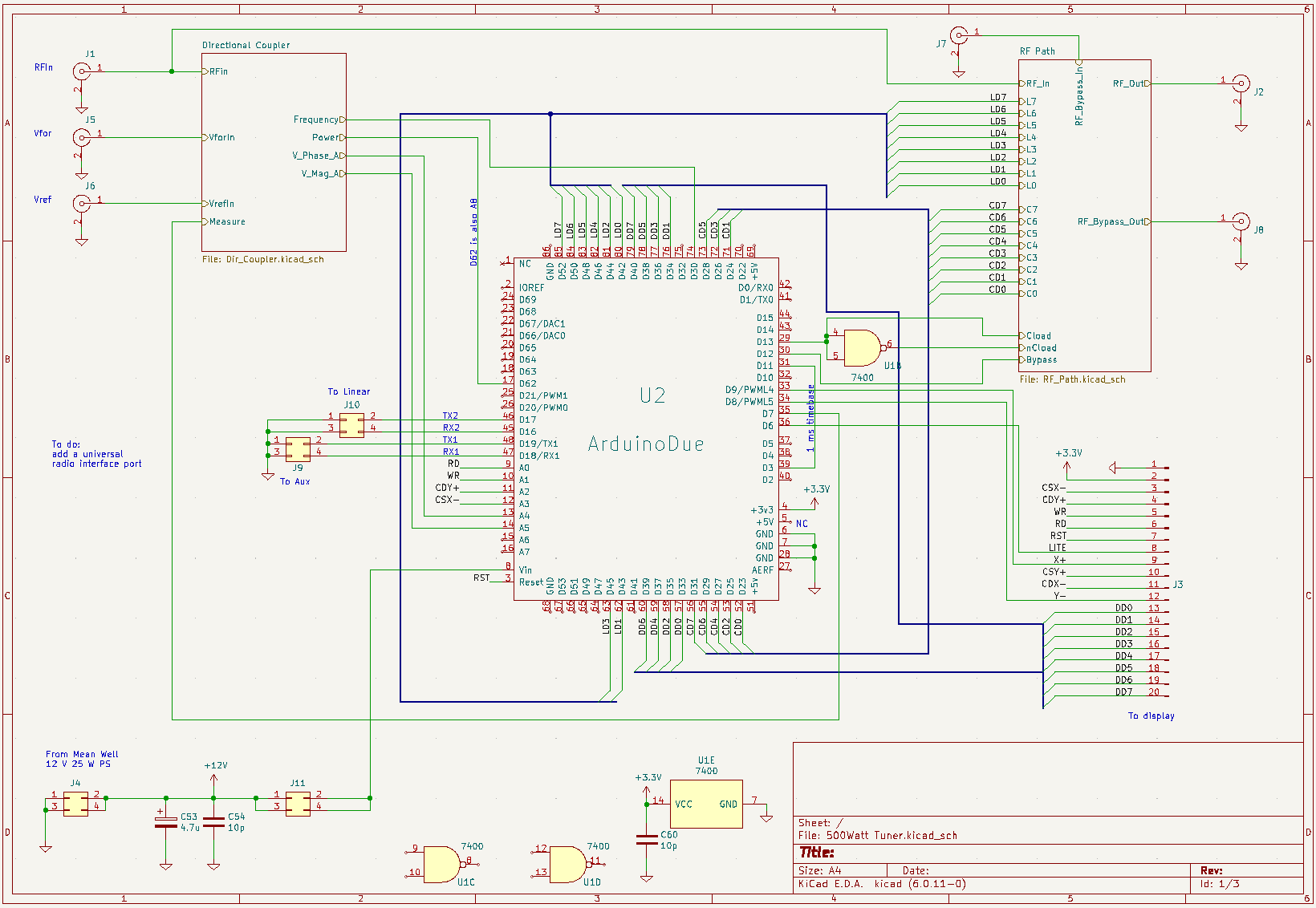
Finally, below is main page.  The function of J11 is to disconnect 12 volts from the Arduino during programming with the lap top.
The two blocks in the upper left and right are the abstraction of the two pages that I have already discussed.  The connector in the lower right is the touch screen display connector (read the Arduino documentation carefully, this interface is a bit tricky).  I also found that when I set the Arduino to read analog inputs using 12 bit A/D, it interferes with the display operation.  So, as soon as the analog input is read, the A/D must be put back into 10 bit mode.  The block in the middle is the Arduino Due.  

If you note, there is a funny arrangement for the bypass connectors.  The reason is that I do not plan to route the bypass RF signal on the PWB (routing got too complicated).  I will have an SMA cable running from one side of the PWB to the other side.  A much simpler solution.  So, J7 and J8 are connected to each other with the SMA jumper. 

The two connectors J5 and J6 connect to the directional coupler as you can see in the prototype picture below.  The two inductors on the right are the voltage (white) and current (blue) sense transformers.  The two cables on the right (the blue side of the directional coupler) are the main RF signals.  The tow SMA cables on the left (white) side are the forward and the reflected signal cables.  This is a prototype of magnitude and phase sensor.


As of now, I have decided not to incorporate a power supply into the package and power the tuner of the Power Pole distribution.  I am feeding the Power Pole with a 20 Amp Astron linear supply that I have owned since the early 90s.  Worst case, I will upgrade the power supply.  The Power Pole can handle up to 40 amps.

And here is the board layout as it stands now:

Saturday, May 13, 2023

Ten Tec Omni D Transceiver Enhancements - Part 3

 I have been using my Ten Tec enhancement box for a bit less than a year.  CW and FT8/FT4 work just fine.  But I have had a lot of complaints about RF on the voice signal.  Some people even though I was being malicious.  That was not going to work.  

I tried a variety of RF mitigation techniques and none of them worked.  

Until...I made two observations.  One was that all power returns in the Ten Tec were routed through the chassis.  The other was that all the voice input paths were isolated from the chassis using an insulator (maybe some sort of phenolic material).   That told me everything I needed to know.  I had made a mistake not isolating the microphone path from the enhancement box chassis.  Even after isolating the microphone path, some of the RFI problem remained.  The most likely path was the sound blaster dongle.

I also encountered a second problem.  The Mean Well 350 watts, 12 volts power supply has a maximum output of 12.6 volts.  The Astron power supply providers about 14.5 volts.  Since the power output of a Class AB amplifier changes by the square of the supply voltage,  one can expect a reduction of about 30% in the power output.  That is exactly what I observed.  70 watts max output rather than 100 watts.

The solution involved two steps:

  • Replace the metal box with an ABS box (at least for now with its own power supply)
  • Go back to the Astron power supply.
As of now, it is working fine and I am getting good reports.


Tuesday, August 16, 2022

500 Watt Antenna Tuner Part 7 - User Interface

I have explored a lot of ideas about the user interface and finally decided to go back to my tried and tested approach and use a tab in my Stationmaster software for the user interface.  It gives me a lot of flexibility.   

At a basic level, I can envision buttons for "measure power", "tune", and "bypass".  When operation of relays is called for, the tuner might come back and ask power to be reduced.  If one of the software controlled radios is in use, the power can be reduced by the software, otherwise, user feedback provided.

If I ever get ambitious, I will display a Smith Chart on the screen and display the path of the tuning on the Smith Chart.  I will see.

For testing, I will use a simple Command Line Interface (CLI) like the one I use in the tuner simulator and I described earlier.

Adjusting Amplifier Power Level


I have three radios, a modern Yaesu FTDX10 and an old Ten Tec Omni D from the 1980s (and a Ten Tec Jupiter that is a new acquisition).  The case for the Yaesu radio is simple, it has a nice API that I am currently using for the contesting interface so I will not discuss it anymore.  For the Ten Tec, it would be good if I don't have to manually reduce the output power (putting 100 watts into a 10:1 SWR would not be great).  Below is the schematic of the Ten Tec ALC circuit (I have used the same reference designations in the Ten Tec manual).  There are two controls in the radio.  The drive which controls the level of the signal (CW or phone) applied to the low level driver and ALC which controls the threshold at which the forward power signal is used to roll back the gain of the low level driver.  The ALC signal is single to the base of Q8 is the rectified output of a Brune bridge fed through a 10K resistor.  


I will have to experiment with injecting current into the base of Q8 also from a 10K source (maybe with a diode blocker so It does not interfere with normal operation) to see if I can automate the output power adjustment.  To implement the idea, I will have to build a new enhancement box for the Ten Tec (https://ad2cc.blogspot.com/2022/04/ten-tec-transceiver-enhancements.html).  This will not be the only enhancement that needs to go in.

In the mean time, I will use the combination of power measurement in the tuner and manual adjustment of the radio to set the desired power level for tuning and for driving the power amp.


500 Watt Antenna Tuner Part 8 - Software and Microcontroller

Controller Hardware and Programming Language Selection

I have experience with Arduino and Raspberry Pi.  I used the Arduino for a telemetry board for our ham radio club EME head end.  I programmed it in C++ (a programming language from Hell).  I use the Raspberry Pi to run my Stationmaster software and it is programmed in Go (as programming languages should be).  Python is the natively supported programming language for Raspberry Pi, but for a lot of reasons which one of them was my naiveté, I decided to use Go (I had also switched from Python to Go as my go to programming language for the most part around 2015 or 2016).  It has worked out handsomely, but I have had to come up with some low level workarounds.

This experience has convinced me of two things.  One is that Arduino is a better solution for the tuner (though Raspberry Pi is a fine solution for more general purpose use cases).  The other is not to try to program it in anything other than its natively supported language and libraries, and that would be C/C++ (though as I have gotten more and more into it, my approach has become C where you can, C++ where you must).

But which model?  I only have an Arduino Due on hand that I am saving for the 500 watt power amp that I will build next.  Given that I have to buy something, I need to decide which one.  My starting selection will be I/O count.  I am not a fan of I/O expanders (more board area, more parts, more interconnections, more interference, more code, more things to go wrong).   So, let me start there:

  • 1 pins for the bypass relay
  • 1 pin for the capacitor relay (across load - Region 1 or across source Region 2 see below)
  • 8 pins for the capacitor network
  • 8 pins for the inductor network
  • 15 pins for the touch screen display
  • 2 analog pins for magnitude and phase of the reflection coefficient
  • 1 analog pin for power level input 
  • 1 pin for frequency input
  • 4 additional pins for other user interface functions that I have not thought of yet
  • 4 spare pins
So, I will need something around 45 I/O pins which puts my in the 54 pin and $40+ space in Arduino land.  So, might as well go with the Due that I have on hand.  I will also get the benefit of 12 bit A/D convertors in place of 10 bit ones as well as nine 32 bit timer channels.  Swinging 3.3 volt digital signals will also generate less noise than swinging 5 volt ones.  

This is a 32 bit ARM core micro controller running at 84 MHz.  That should make many things easier.  It has 3.3 volt IO pins, so the interfacing will need some extra care.  It takes in 6-12 volts input and generates +3.3 volts output at 800 mA (it also generates +5 volts at 800 mA but it is not likely that we will need it).  It has an Analog Reference input (AREF) which I might want to drive from the 1.8 volts stable output of the AD8302 for a more accurate A/D conversion.

User Interface 

For user interface, I have decided to use the Adafruit 3.5" TFT touch screen display.  When I first started thinking about the user interface, I was not sure what I wanted to do so a touch screen display seemed to be a natural choice because of its flexibility.  As I worked on ideas about how to use the touch screen display, I decided that it was the best option since it simplified the design and provided flexibility for any future improvements.

Software Design


The structure of the software is a state machine.  The state transition diagram is shown here:

StateEntry CriteriaActionNext State
POWERONPower onMonitor buttonsPRETUNE or PREBP
PRETUNEPress TUNEMeasure powerRFLOW, RFHIGH, MEASURE
RFLOWPower level lowIncrease powerPRETUNE
RFHIGHPower level highDecrease powerPRETUNE
MEASUREPower in rangeMeasure Freq, GammaTUNE
TUNEAutomaticCalc/Apply C and LMONITOR
MONITORSuccess tuningMonitor SWR, PWR, buttonsPRETUNE, PREBP
NOTUNEError detectedCorrect errorPRETUNE, PREBP
PREBPPress BYPASSMeasure powerRFHIGHBP or BYPASS
RFHIGHBPPower highDecrease powerPREBP
BYPASSPower in rangeActivate bypass relaysPRETUNE

The state machine enters the POWERON state upon the application of power and looks for a button push.  If the TUNE button is pushed (BYPASS button discussed below), it enters the PRETUNE state and in this state measures the RF power at the input.  If the power is less than the required threshold (to be determined experimentally) for successful tuning, it enters the RFLOW  state and instructs the user to increase the power and push the DONE button which will move the state machine back to the PRETUNE state.  If the power entering the tuner is too high for safe tuning (minding our on the air manners and following good practice), it enters RFHIGH state and instructs the user to decrease the power and push the DONE button which will move the state machine back to the PRETUNE state and restarts the cycle.  If the power level is in the correct range, the state machine transitions from the PRETUNE state to the MEASRE state where it measures the phase and magnitude of the reflection coefficient (Gamma) and the frequency of the incoming signal.  After the measurement is complete, it transitions to the TUNE state.

In the TUNE state, the controller calculates the required capacitor and inductor values using the equations discussed in the "Tuning Algorithm" page.  Because the Analog Devices phase output has a 180 degree phase ambiguity, and under some conditions it might not be possible to resolve this ambiguity as discussed earlier, two sets of capacitors and inductors may have to be calculated and tested to determine the right match.  After the relays for the desired capacitor and inductor combinations are activated, the reflection coefficient is measured.  If SWR is in the desired range (currently assumed to be 1.2), the controller enters the MONITOR state.  In this state, it measures and displays PWR and SWR data on the touch screen.  It also monitors the TUNE and BYPASS buttons and depending on which button is pushed, it moves to PRETUNE or PREBP state respectively.

Assuming that I can manipulate the Ten Tec ALC circuit, some of the power up and power down cases might be achievable automatically.  But that is a future project.  I just need to make allowance for it.

I should note that I do not plan to operate the relays with the power applied.  I have built and tested a serial link between the tuner and the Stationmaster software.  I plan to ask for key down when I need to make a measurement and then ask for key up before operating the relays.  The reason I have the RFLOW and RFHIGH states is that below a certain power level, it will not be possible to make good measurements and too high of a power level for tuning is in general bad on the air manner and under high SWR conditions, bad practice.

If the SWR measurement is above the desired limit, it enters the NOTUNE state.  This is an error state and I will experimentally determine what to do next.

If in the POWERON state (or any other state where the buttons are monitored) the BYPASS button is pushed, the state machine moves to the PREBP state and in this state measures the input power to the tuner.  If the power is too high for a given SWR, it moves to the RFHIGHBP state and instructs the user to lower the power and push the DONE button which moves the state machine back to the PREBP state and repeats the cycle.  If the power is at a safe limit, it will move to the BYPASS state and operate the bypass relays.  In this state, it monitors and displays the PWR and SWR levels and monitors the TUNE and BYPASS  buttons and depending on which button is pushed, it moves to PRETUNE or PREBP state respectively.

When the state machine is in the MONITOR state, the tune button changes its color from white to green.  When it is in the BYPASS state, the bypass button changes its color from white to green.

User Interface Screenshots

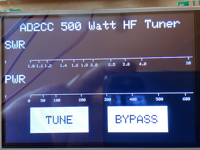
As of now, here are my ideas about the user screens.  I might modify them as I build and test the tuner.  Ignore the 10 and 30 watt limits, they will change.


Basic Tuner Screen


Tuner Instructing the Power to be Lowered


Tuner Instructing the Power to be Increased


Tuner in the Tuned State


Tuner in the Bypass State

Frequency Measurement

It took me a few days of investigation, testing and trial and error to figure out how to measure frequency, but it worked.  In the Arduino Due microcontroller, all signals are sampled by the master clock (84 MHz) before being processed, so the frequency has to be at least 2.5 times less than the master clock frequency.  If I limit myself to HF bands only, I don't need to do anything other than to attenuate the output, put it through a comparator (that I will disable when not measuring frequency, less digital noise that way), and input it to the Arduino Due.  The reason being that 84/30 = 2.8 > 2.5; so I am in good shape.  If I want to go up to the 6 meter band, I will have to put 2:1 divider in the path (54/2 = 27) and I will end up in about the same place (84/27 = 3.1 > 2.5).  I need to think about this (I decided to stick to the HF band - 6 meter will have many more challenges and I don't feel up to them at this time).

Here is how I went about building the proof of concept.
  • The lower numbered timer-counter (TC0) is used for the operating system functions. For example, if call the "delay" function, chances are that the operating system is going to use the timer for it.  If you are going to use any other library, it would be good to check if the library uses any of the timers-counters.
  • The timer-counters have a number of input and output signals.  The signals are multiplexed with most likely one other peripheral signal and then multiplexed with general purpose I/O pins.  Some of these pins do not make it out to the Arduino pins.  Some may be multiplexed with other needed pins.  So I had to make a study of it.  That rules out all three channels of the timer-counter one (TC1).
  • I ended up using timer-counter two (TC2) for my testing.  I used channel 0 to generate the test signal.  The highest frequency that it can generate is 21 MHz because the highest frequency clock available to the timer-counters is master clock divided by two so the highest frequency that the timer can generate is 1 tick low and 1 tick high, hence master clock divided by 4.
  • TC2 Channel 0 toggles the TIOA6 signal (see table 36-4 of the microcontroller data sheet) every time there is match with register A and register B (they are both loaded with 1).  TIOA6 signal is connected to the I/O line PC25 in group B peripherals.  On the Due schematic, it is labeled PWM5 and connected to pin 5 so labeled on the board and the connector.  This is the clock input to channel 2 of the same TC2 (more on this in a few lines).
  • I used channel 1 to generate 1 millisecond timebase by driving it by the highest frequency clock available to the timer (42 MHz) to minimize phase ambiguity as much as possible.
  • The millisecond timebase pulse is output on signal TIOA7 which is routed to controller pin PC28, also in peripheral B.  On the Due schematic, PC28 is labeled PWM3 which appears on pin 3 of the board (and it is so labeled).
  • I verified both the clock frequency of pin 5 and the 1 ms pulse on pin 3 on a scope.
  • I drove channel 2 with the test signal and stored the value of the counter in register A (RA) on the rising edge of the clock and the value of the counter in register B (RB) and generated an interrupt on the falling edge of clock
  • Clock input input to channel 2 of TC2 is signal TCLK8 which appears on the controller pin PD9 and on the Due schematic is labeled PIN30 and it appears on the board pin 30.
  • So, the wiring is a jumper from pin 5 of the Arduino (clock output of channel 0 - the test frequency) to pin 30 (clock input of channel 2 of TC0).  The other jumper is from pin 3 (1 ms timebase) to pin 11 of the Due (signal name PWM11) which is pin PD7 of the controller and from table 36-4, we see that it is signal TIOA8 which loads register A on its rising edge and register B on its falling edge.  The difference is the number of pulses that channel 2 has seen in a millisecond.
  • The interrupt service routine (which cannot have any arguments or return any value) calculates RB-RA which I use to calculate the frequency. 
Some of the resources that one might find useful are:

The SAM3X microcontroller data sheet (actually a book, it is 1,459 pages).  

A tutorial by KO7M that helped start me in the right direction.

The Arduino Due schematic on the Due webpage is needed to trace signals from the source (data sheet) to the useable end point (Due board connector and pin number).

I ended up digging through three software modules and reading code to figure out what it did.  The three were:
  • Power Management Controller (PMC) - it contains some of the clock action
  • Parallel Input/Output Controller (PIO) - that is where all the multiplexing happens
  • Timer Counter (TC) - That is where the 3 TC modules with their 3 channels are located

The old Arduino IDE did not add these libraries automatically, so I had to add them manually.  On my mac, they are stored in (the new one does):

$HOME/Library/Arduino15/packages/arduino/hardware/sam/1.6.12/system/libsam/include

The software is in a preliminary state with stubs and test scaffolding, but the core functionality as described can be found here.